1. The purpose of PCB process selection
With the development of electronic technology, printed circuit boards have gradually developed from single-sided boards to double-sided boards, multi-layer boards, flexible boards and rigid-flex boards. The manufacturing and processing technology continues to move towards high precision, high density, fine aperture, and fine aperture. The development of wires, small pitch, high reliability, multi-layer, light weight, and thin profile. The technical content of printed circuit board processing is getting higher and higher, and the technical difficulty is getting more and more difficult. The performance and quality of printed circuit boards are beginning to become Important factors affecting the performance, quality and reliability of electronic products.
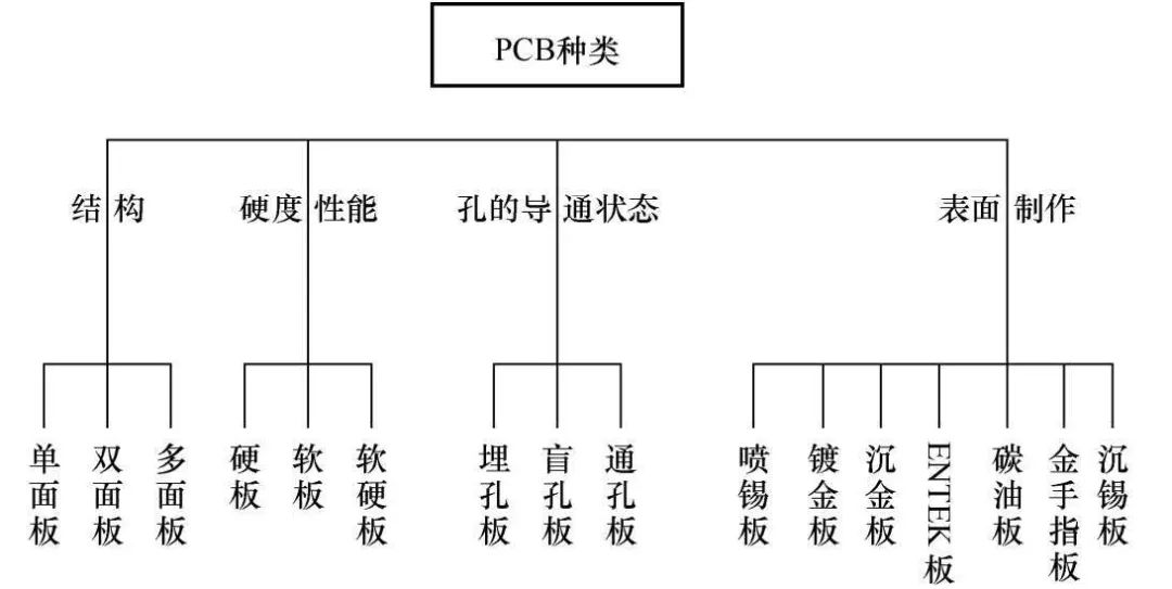
Common PCB types are shown in the figure.
In fact, the performance and quality of the printed circuit board are related to the structure type of the printed circuit board, the choice of base material, and the processing technology. Different types (rigidity and flexibility) and different structures (single-sided, double-sided, multi-layer) , The performance indicators of different substrates are different. Therefore, the purpose of the printed circuit board process selection is to determine the various indicators and parameters of the printed circuit board according to the performance and quality requirements of the electronic product, combined with the subsequent assembly process, to ensure the performance and quality of the electronic product.
2. Classification and Introduction of PCB Commonly Used in Electronic Assembly
Depending on the structure, performance level, material, and application, PCBs can be classified in a variety of ways, which are briefly introduced below.
3.1 Classification by structure
Printed circuit boards can be divided into the following four basic types according to their structure.
(1) Single panel
Single-sided board refers to the conductive pattern on only one side of the printed board. In this type of printed circuit board, the components are concentrated on one side, and the wires are concentrated on the other side. Because the wires only appear on one side, this kind of PCB is called a single-sided (Single-sided).
Single-sided boards have many strict restrictions on the design of the circuit (because there is only one side, the wiring cannot cross, and it must go around a separate path), and it is rarely used now.
(2) Double panel
Double-sided board means that there are conductive patterns on both sides of the printed board. The printed board with this structure has wires on both sides, and the double-sided wires are interconnected through metal vias. The wiring area of the double-sided board is twice as large as that of the single-sided board. The double-sided board solves the difficulty of interleaving wiring in the single-sided board (it can be connected to the other side through via holes), and is suitable for more complicated circuits.
(3) Multilayer board
Multi-layer boards refer to printed boards with at least 4 or more conductive pattern layers connected to each other. The layers are separated by insulating materials and formed after bonding and hot pressing. The use of multi-layer printed boards is to further increase the effective wiring area. Usually one double-sided board is used as the inner layer, two single-sided boards are used as the outer layer, or two double-sided boards are used as the inner layer and two single-sided boards are used as the outer layer. The positioning system and the insulating bonding material are interconnected, and the conductive patterns are interconnected according to the design requirements. It is worth noting that the number of layers of the board does not mean that there are several independent wiring layers, because in special cases empty layers are added to control the thickness of the board, usually the number of layers is even, and the outermost two layers are included. At present, most common desktop computing motherboards have a structure of 4 to 8 layers. Some large supercomputer motherboards can have more than 40 layers. In addition, in theory, multi-layer boards can achieve nearly 100 layers.
(4) Flexible printed circuit board
A flexible printed circuit board is a flexible printed circuit board (Flexible Printed Circuit Board, FPC), also known as a flexible printed circuit board or a flexible printed circuit board. According to the definition of IPC, a flexible printed board refers to a product that is designed and manufactured on a flexible substrate by means of printing. Compared with rigid printed boards, flexible printed boards have a high degree of flexibility. They can be bent, wound, twisted, and folded freely, and can be wired three-dimensionally. They can be arranged and changed in shape according to the space layout requirements. Any movement and expansion inside can achieve the effect of component assembly and wire connection integration, which is an important basic support for the development of electronic products in the direction of high density, miniaturization, light weight, thinness, and high reliability.
The flexible printed circuit board also has excellent electrical properties, high temperature resistance, flame resistance, stable chemical properties, and good stability. Its use provides great convenience for circuit design and machine assembly. At present, flexible printed circuit boards have been widely used in electronic products, especially high-end electronic products, such as notebook computers, smart phones, military instruments and equipment, automotive instrument circuits, cameras, etc. The biggest disadvantage of flexible printed boards is that their mechanical rigidity is not enough. However, through the use of reinforced materials or a rigid-flex board design with a combination of soft and hard, the problem of weak load-bearing capacity can be better solved. The future of flexible printed boards The scope of application and development prospects will get better and better.